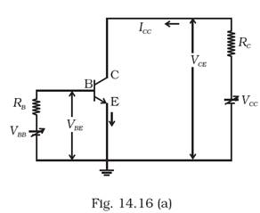
Consider the circuit arrangement shown in Fig 14.16 (a) for studying input and output characteristics of n-p-n transistor in CE configuration.
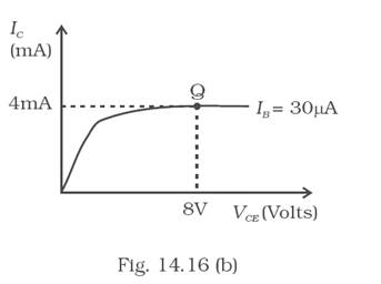
Select the values of RB and RC for a transistor whose VBE = 0.7 V, so that the transistor is operating at point Q as shown in the characteristics shown in Fig. 14.16 (b).
Given that the input impedance of the transistor is very small and VCC = VBB = 16 V, also find the voltage gain and power gain of circuit making appropriate assumptions.
Circuit Diagram:
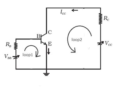
Using KVL at loop1,
![]()
![]()
Putting the value from the curve,
![]()
![]()
Using KVL in loop2,
![]()
![]()
Putting the values from the curve,
![]()
![]()
The voltage gain will be,
![]()
![]()
The power gain will be
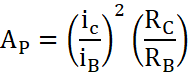
![]()
1